
Right. That’s how most people pronounce the name of a field programmable gate array.
But – what’s an FPGA good for, you might wonder. Glad you asked…
Conceptually, an FPGA is a pile (a BIG pile!) of identical logical units (let’s assume they are all NOR-gates) that can be wired in whatever way the person designing the content of the device wishes. Anything. Really. Without having to resort to a soldering iron. Just like that, in a nice and comfy editor.
Given the recipy made in said editor, the FPGA becomes the logical network you specified. You can design your own boolean logic, counter, memory address decoder or timer (for that, add a clock input). Or imagine wiring up what would probably amount to an entire shopping bag of TTLs to create – say – a simple processor core. Afterall, central processing units are made up of just that; a whole lot of digital logic circuits.
Super – tinkerer’s heaven. Now, I’ve had my eye on these little buggers for a while, but as it was, their pricing was simply prohibitive. The market for many-times-reprogrammable logic is small. Simply because most mass-market-manufacturers go ASIC, using reprogrammable logic only within the confines of their R&D department. They don’t need the reprogrammability in their finished goods. So; with small numbers come high prices; it was a no-go for me. But times change, and – well, either I’ve become richer, prices have dropped or both. The point is; reading Chris Fenton’s article on building a DIY Cray-1 vintage supercomputer, it got me going. I checked out the market, found that beginner-friendly FPCA evaluation/student-kits were now down to what would compare to 10 McDonalds-meals and decided I’d give it a go.
Digilent offers the Arty A7 development board, containing a Xilinx Artix-7 FPGA, powersupply, a few buttons and LEDs, an ethernet port, Arduino-shield-connectors and four proprietary-formfactor-GPIO ports. To go with the board, Xilinx offers a board-locked toolchain at no cost. Super – just what I wanted. So, ‘Click here to buy’ on that one and a couple of little add-on-modules for the GPIO-ports, to enable me to setup something functional; an RS232 port and a tiny OLED-display-module.
While waiting for the mailman, I looked around for learning material, ordered a preowned book on the subject and watched some Youtube-videos. I learnt that FPGAs have come a long way from what was said about their functionality above.
Today, FPGAs come with built-in hardware ADCs, clock circuitry and a whole slew of other bits and bobs enabling developers to create not only digital circuitry, but whole SoCs, rivalling your average microcontroller in functionality. Add to that the fact that FPGA manufacturers have now devised a way of providing software-modules implementing Ethernet-ports, USB-ports, ADC-modules and even processor-cores. Remember that shopping bag of TTLs i talked about earlier? It’s now drag-and-drop…
The mail arrived and I set about installing the toolchain. Which required me to go get a bigger SSD. It appears that all this nice modularity and graphical desigh razzmatazz bloats what was once a simple editor/compiler function into something that devours no less than 50GB and requires you to consider how many of your CPUs cores you can dedicate to the compile-process – which can last for minutes once started.
I instantly got lost in the toolchain. It’s radically different from what I’m used to do. More like designing hardware, actually. Think Kicad or Orcad.
So, I turned to youtube-tutorials. Hmmm. A mixed bag.
Proper tutorials, made by Digilent, then? Again, a mixed bag. The usual version-I-have-differs-from-version-used-in-tutorial crap. I’ve managed to follow most of a tutorial, creating a ‘simple’ design holding some GPIO, a UART and a MicroBlazeTM soft-CPU. I believe I’ve done it right, but the tutorial lost me when I was told to transfer the ‘hardware design’ over to the part of Xilinx’ toolchain responsible for writing the code to said soft-CPU. Because obviously, the CPU needs a program to do something meaningful with the ‘hardware’.
I end up with a .xsa file, supposedly containing the logic design. But the menu item I’m supposed to activate isn’t there:
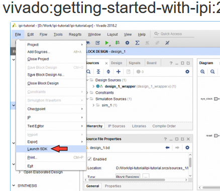
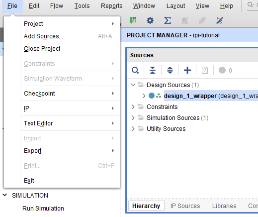
It seems the tool changed its name from Vivado SDK to – presumably – Vitis. And Vitis offers little in the form of clues on how to import the design, meaning I’m by now stuck in no-mans-land.
So, I’ve opened up an account on Digilent’s forums. Next step will be to write a structured question and hope for a structured answer.